E-Paper



India launches first advanced 3D glass chip unit in Odisha
Odisha's CM laid the foundation for India's first glass substrate chip packaging unit, advancing local semiconductor technology and reducing import dependence.

 Prefer HTon Google


India moved a step closer to ending its dependence on imported chip packaging technology on Sunday, with Odisha Chief Minister Mohan Majhi laying the foundation stone for the country’s first glass substrate-based advanced chip packaging unit in Bhubaneswar that promises to bring cutting-edge semiconductor packaging capability onshore for critical sectors ranging from artificial intelligence to defence.
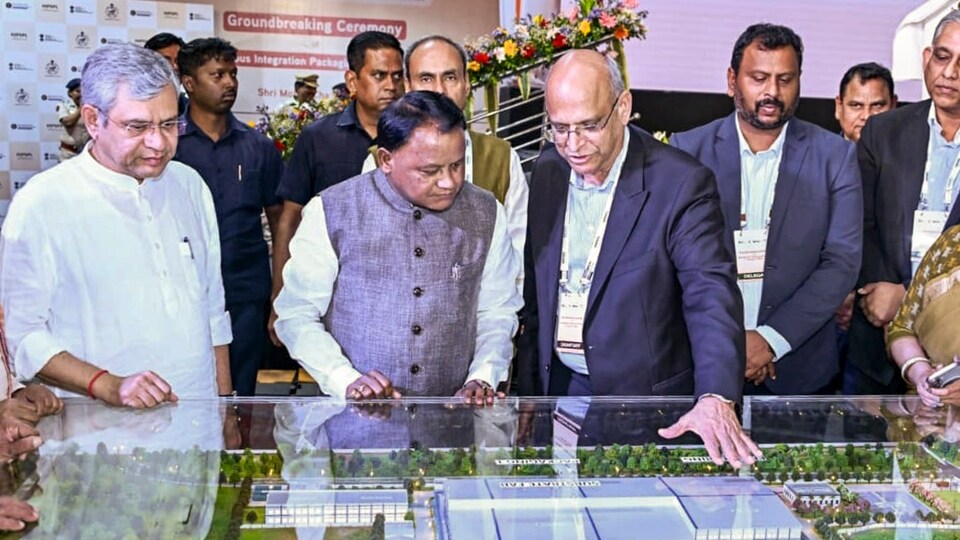
The facility, being set up by US-based 3D Glass Solutions Inc. (3DGS) at Info Valley in Bhubaneswar, entails an investment of approximately ₹1,943 crore and will deploy advanced 3D heterogeneous integration (3DHI) packaging technology which India has so far relied on imports to access.
Union Electronics and IT Minister Ashwini Vaishnaw, who attended the groundbreaking alongside state IT Minister Mukesh Mahaling, called it “a historical day” for Odisha. “The state is diversifying from metals and minerals to many new industrial bases,” Vaishnaw said, pointing to Odisha’s emergence as both an IT hub and an electronics manufacturing destination.
“A high-tech industry coming to Odisha is a matter of pride. This is an advanced technology. Normally, a silicone substrate is used in the manufacturing of chips, and now the technology of advanced 3D Glass substrate will be used, and the foundation stone of the first major plant using that technology has been laid in Odisha. We will also work to double the capacity of the plant after the completion of the first phase of the plant,” said Vaishnaw.
The vertically integrated unit will package semiconductor chips for high-stakes applications including artificial intelligence, 5G networks, defence systems, data centres, and high-performance computing. At scale, the facility is designed to produce 69,600 glass panel substrates, 50 million assembled units, and 13,200 3DHI modules annually. It is expected to generate over 2,500 direct and indirect jobs.
The technology stack centred on glass interposers and embedded glass substrates represents a significant leap from conventional organic packaging, offering better thermal performance and higher integration density critical for AI-grade chips.
The 3DGS plant is the second semiconductor facility to break ground in Odisha within months. SiCSem Private Limited, in collaboration with UK-based Clas-SiC Wafer Fab Ltd., is already building India’s first commercial silicon carbide (SiC) fabrication unit at the same Info Valley campus targeting annual output of 60,000 wafers and 96 million packaged units for electric vehicles, railways, defence, and renewable energy.
The union cabinet had approved both Odisha projects in 2025 as part of a broader push that has greenlit 10 semiconductor projects nationwide, with cumulative investments exceeding ₹1.6 lakh crore.
The 3DGS and SiCSem approvals are part of India’s larger ambition to build a self-reliant semiconductor ecosystem and reduce dependence on chip imports.