"Now our chips, coming out of India's plants, have started reaching customers in the country and the world," Prime Minister Narendra Modi said on Thursday, inaugurating the fifth edition of the Semicon India conference in New Delhi. Pitching India as a trusted alternative for global manufacturing, he said the country was "taking every step needed to become a preferred destination for the semiconductor industry".
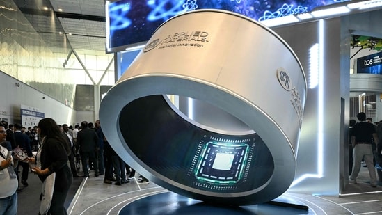
The first phase of India's semiconductor programme has moved from approvals and construction to commercial production. Five of the 12 projects approved under the India Semiconductor Mission (ISM) 1.0 now produce chips or packaged semiconductor products, and the other seven are at various stages of construction and development. All five producing units are packaging plants; the programme's three fabs, where the chips themselves are made, are expected to start production between 2027 and 2029.
At the event, Modi virtually inaugurated Suchi Semicon's facility in Surat, Gujarat, and CDIL's facility in Mohali, Punjab, both of which began commercial production on Thursday.
The 12 projects, approved between 2023 and 2026, represent an investment of more than ₹1.64 lakh crore. The government classifies them as one silicon fab, one silicon-carbide fab, one integrated gallium-nitride (GaN) Micro-LED fab and nine packaging units.
How advanced are India's chips?
Fabs etch circuits onto silicon wafers at a given node. The node, measured in nanometres (nm), denotes a generation of manufacturing technology; the smaller the number, the more densely transistors are packed on a chip and the more capable it is. The world's most advanced processors are made at 3nm and 2nm --- Apple’s A20pro chips on its latest iPhones, for instance, are 2nm.
{{/usCountry}}Fabs etch circuits onto silicon wafers at a given node. The node, measured in nanometres (nm), denotes a generation of manufacturing technology; the smaller the number, the more densely transistors are packed on a chip and the more capable it is. The world's most advanced processors are made at 3nm and 2nm --- Apple’s A20pro chips on its latest iPhones, for instance, are 2nm.
{{/usCountry}}India's own chipmaking is at far larger nodes. The state-owned Semi-Conductor Laboratory (SCL) in Mohali, which the government describes as the only facility in the country that can handle the whole chipmaking process from design to testing, runs a 180nm production line and is being upgraded to cover nodes from 28nm to 180nm. Nodes do not apply to packaging plants such as the five now in commercial production. The most advanced node in the ISM 1.0 pipeline is 28nm, at the Tata-PSMC fab in Dholera, which will become India's most sophisticated chipmaking facility once it starts production.
The government has said it has chosen to start with mature nodes, which supply chips for cars, power systems, industrial equipment and consumer electronics, and to use them to build up plants, suppliers and a trained workforce before moving to more advanced manufacturing and research.
The second phase of the mission, ISM 2.0, is meant to take that step. Its plans include a roadmap to the 3nm and 2nm nodes and support for at least 50 fabless companies, which design chips and outsource their manufacture.
Also read: Semincon India 2026: Road to semiconductor self-reliance
1. Tata-PSMC: India's first large silicon fab
The largest project, and the only silicon fab, is Tata Electronics' ₹91,526-crore plant in Dholera, Gujarat, which Tata is building with Taiwan's Powerchip Semiconductor Manufacturing Corporation (PSMC). The fab is designed to make chips at the 28nm, 40nm, 55nm and 110nm nodes, with planned capacity of 50,000 300mm wafers a month.
The most advanced node publicly specified for the project, 28nm, is a mature process, several generations older than the 3nm and 2nm processes used for the most advanced chips, but chips made at these nodes go into cars, industrial equipment, power-management systems, connectivity devices and consumer electronics.
Earlier government and company press releases indicated the fab would be operational by the end of 2026; current project reporting puts commercial production around 2028. Tata Electronics CEO and managing director Randhir Thakur said at the Semicon event on Thursday that the Dholera fab and the company's packaging facility in Assam were on track.
2. SiCSem: silicon-carbide chips for power applications
The ₹2,066-crore SiCSem project in Bhubaneswar, Odisha, will be India's first commercial silicon-carbide fab. Silicon carbide is a compound semiconductor made of more than one element, and it handles higher voltages and temperatures than ordinary silicon, making it suitable for power electronics. The facility, being set up with UK-based Clas-SiC Wafer Fab, will have capacity for 60,000 wafers a year and packaging capacity of 96 million units a year. Its chips are meant for EVs, fast chargers, solar inverters, railways, defence and data-centre power systems.
Production is targeted for 2027-28.
3. Crystal Matrix: GaN and Micro-LEDs
Crystal Matrix, approved in May 2026, is setting up another specialised fab in Dholera: an integrated gallium-nitride compound-semiconductor fabrication facility with an assembly, testing, marking and packaging (ATMP) unit. It will offer GaN foundry services, making chips to other companies' designs, and epitaxy, growing thin crystal layers, on six-inch wafers.
The plant will make Mini- and Micro-LED display modules for large commercial displays, TVs, smartphones, vehicle displays, extended-reality (XR) glasses and smartwatches. Planned capacity is 72,000 square metres of Mini/Micro-LED display panels and 24,000 sets of RGB GaN epitaxy wafers a year. The project is in the development stage, and production is expected to begin around 2029.
The other nine projects, which the government classifies as packaging units, are outsourced semiconductor assembly and test (OSAT) or ATMP facilities. They take dies, the individual chips cut from finished wafers, made elsewhere and assemble, package and test them.
4. Micron's Sanand facility
US memory-chip maker Micron's unit in Sanand, Gujarat, began commercial production on February 28, 2026. It assembles and tests DRAM and NAND chips, used respectively for a device's working memory and its storage, from wafers made in Micron's global manufacturing network.
Micron expects output to rise from tens of millions of chips in 2026 to hundreds of millions in 2027.
5. Kaynes Semicon's Sanand plant
Kaynes Semicon's plant began production on March 31, 2026. Its initial products include intelligent power modules (IPMs), which combine semiconductor devices for power-management applications. The facility can make more than 6.33 million chips a day and is aimed at domestic and international markets.
6. CG Semi's OSAT facility
CG Semi, a joint venture of CG Power, Japan's Renesas and Thailand's Stars Microelectronics, began commercial production in July 2026 at its unit in Sanand, Gujarat, which Modi inaugurated.
The plant can turn out up to 300 million semiconductor units a year at peak capacity, for chips used in automotive, industrial, consumer, power and communications applications.
Also read: Delhi’s semiconductor policy eyes R&D, manufacturing
7. Tata Semiconductor Assembly and Test (TSAT)
Tata is building a ₹27,120-crore facility in Morigaon, Assam, with planned capacity of 48 million units a day. It will use advanced packaging technologies, including flip-chip, in which a die is mounted face-down and wired to its package through small metal bumps, and integrated system-in-package (ISIP), which combines several chips in one package.
The facility is intended for automotive, EV, telecom and consumer applications. It remains under construction, and production is expected in the near term.
8. HCL-Foxconn's Jewar project
HCL-Foxconn's plant in Jewar, Uttar Pradesh, will make display-driver integrated circuits (DDICs), the chips that control the pixels on a screen, using gold-bump technology. It will have a capacity of 20,000 wafers a month, or 36 million chips a month, for mobile phones, laptops, PCs, automobiles and other displays.
Construction began after a February 2026 groundbreaking, and production is expected to start in 2027.
9. 3D Glass Solutions' Odisha project
US-based 3D Glass Solutions is building the second ISM project in Odisha, after SiCSem, focused on advanced packaging. The facility will produce 69,600 glass panels, 50 million assembled units and 13,200 3D heterogeneous integration (3DHI) modules a year. 3DHI stacks or combines different kinds of chips in a single package. The project is expected to create more than 2,500 direct and indirect jobs.
Its technologies are aimed at AI, high-performance computing, 5G/6G, automotive radar, defence, aerospace and photonics.
Commercial production is expected by August 2028, with full-scale volume production targeted for August 2030.
10. CDIL Mohali
Continental Device India Ltd (CDIL) is expanding its existing semiconductor operations to make high-power discrete devices, including MOSFETs, IGBTs, Schottky diodes and other transistors, in both silicon and silicon carbide. A discrete device performs a single function, such as switching current, whereas an integrated circuit packs many onto one chip.
As power semiconductors, these devices are classed outside the digital logic nodes used for processors. Applications include EVs, charging infrastructure, renewable energy, industrial systems and telecom.
The ISM-backed facility began commercial production on Thursday.
11. ASIP Technologies' Andhra Pradesh project
ASIP Technologies is setting up an OSAT facility in Andhra Pradesh with South Korea's APACT, with an annual capacity of 96 million units for chips used in mobile phones, set-top boxes, automotive electronics and consumer products. The project is under development.
12. Suchi Semicon's Surat facility
Suchi Semicon's OSAT unit for discrete semiconductors, approved in May 2026, has a planned capacity of 1.033 billion chips a year. Its target applications include power electronics, analogue ICs, industrial automation, automotive and consumer electronics.
It began commercial production on Thursday.