E-Paper



Cabinet clears 2 new chip units in Gujarat worth ₹3,936 crore
The government has completed the initial slate of projects under ISM 1.0, taking the total to 12 units and cumulative investments of ₹1.65 lakh crore, Vaishnaw said

 Prefer HTon Google


The Union Cabinet on Tuesday cleared the last two semiconductor units under the first phase of the government’s semiconductor mission, with an investment of ₹3,936 crore. The projects will be funded under the ₹76,000 crore outlay earmarked for the India Semiconductor Mission 1.0, introduced in 2022.
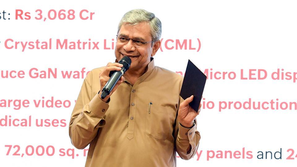
Both facilities, announced by IT Minister Ashwini Vaishnaw during the cabinet briefing, will be set up in Gujarat.
With these approvals, the government has completed the initial slate of projects under ISM 1.0, taking the total to 12 units and cumulative investments of ₹1.65 lakh crore, Vaishnaw said.
The government is now preparing to roll out the next phase, ISM 2.0, which is expected to have an outlay of over ₹1 lakh crore, HT reported earlier.
The government is positioning the larger of the two facilities—Dholera-based Crystal Matrix project—within a broader shift in display technologies from LCD to next-generation MicroLED. For decades, LCD manufacturing was dominated by Japan, South Korea and Taiwan, before China scaled up investments and took global leadership, said Vaishnaw.
With LCD now considered a mature technology, the focus has moved to MicroLED, where India is seeking to build an early presence.
The ₹3,068 crore Crystal Matrix facility will manufacture gallium nitride (GaN) wafers used in Mini and MicroLED displays, along with advanced packaging (ATMP). These components are used in applications such as large video walls, AR/VR systems, studio production, and specialised defence and medical displays.
The project is part of India’s attempt to enter a segment that is still evolving globally, with players like Sony and Samsung leading the way.